- ultra-high throughput spectrometer including a peltier-cooled – temperature 2 – 400 K
- magnetic fields of up to 15 T
- 532nm and 633 nm excitation wavelength
- back-illuminated CCD
Facility Type: Special methods
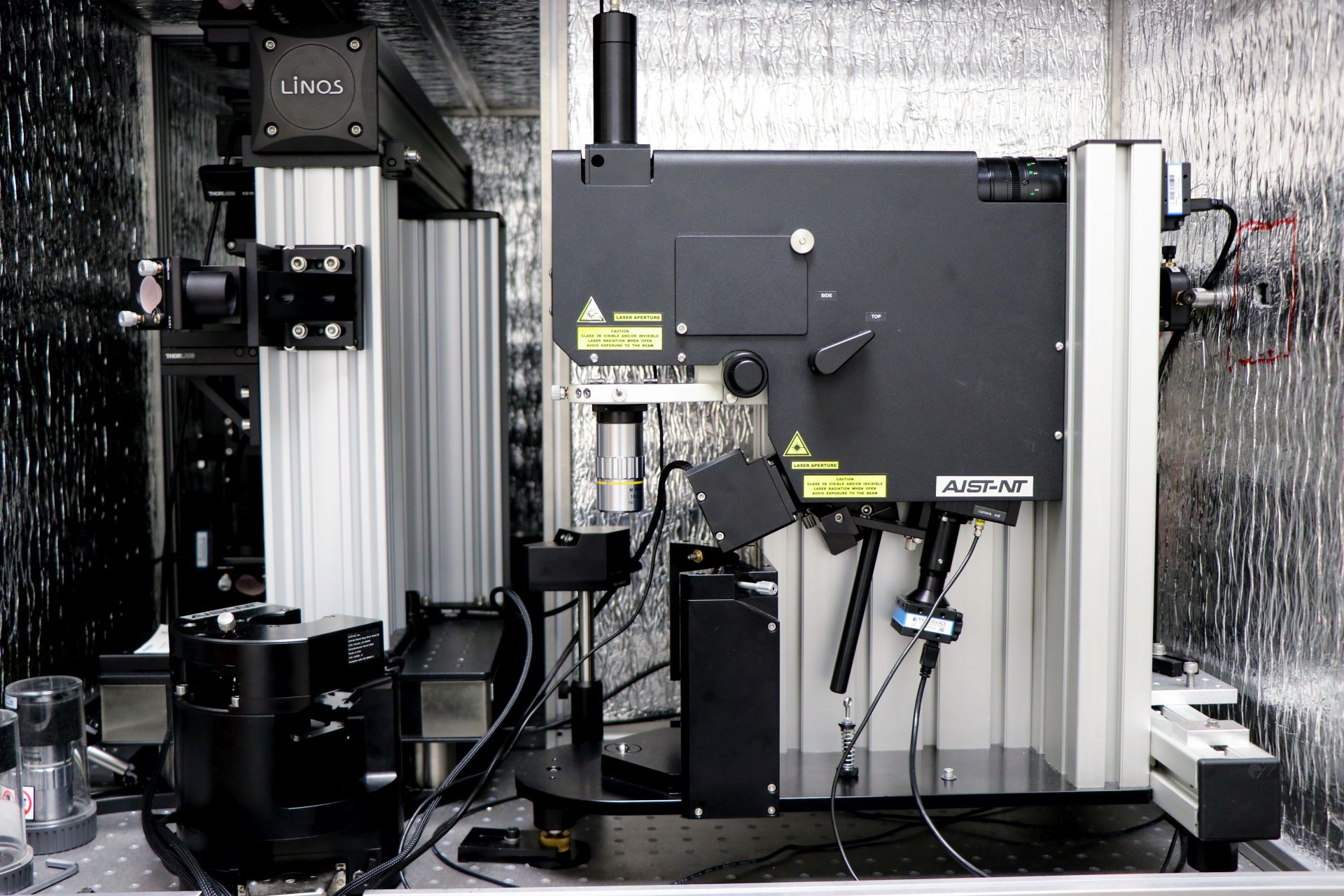
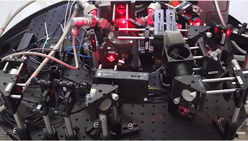
Integrated SPM with Raman spectrometer HR Evo Nano
- LabRAM HR Evolution (Horiba) – 800 focal length Raman spectrometer
- Available excitation wavelengths: 532 and 633 nm
- Coupling to Smart SPM (AIST-NT) for top and side optical access
- High frequency sample piezo scanning for enhanced stability
- Coupling to modular TRIOS/Combiscope SPM platform for top, bottom and side access
- XYZ objective piezo scanner for independent laser scanning
- Fully integrated software for controlling the whole AFM-Raman setup
— Installed 2018 —
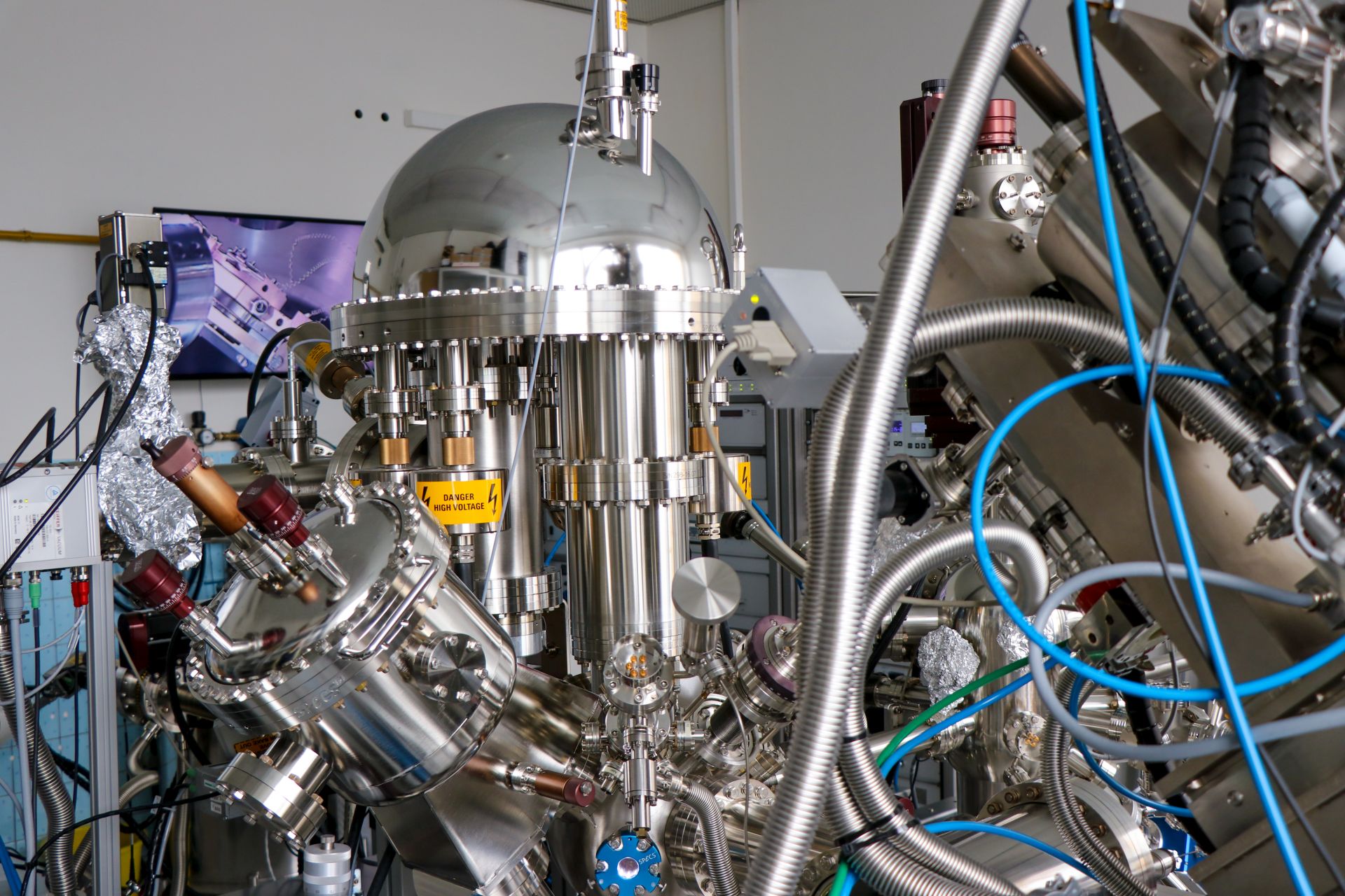
Apparatus for complex study of thin films, interfaces and surface nanostructures
- ultrahigh vacuum apparatus for characterization of the studied samples by methods of X-ray photoelectron spectroscopy (XPS)
- ultraviolet photoelectron spectroscopy (UPS)
- low energy electron diffraction (LEED)
- scanning probe microscopy (SPM)
- low energy ion scattering spectroscopy (LEIS)
- angle resolved photoelectron spectroscopy (ARPES) with 3D spin detector.
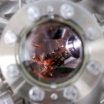
System of four interconnected vacuum chambers (SPECS) separated by gate valves pumped by turbomolecular and ion pumps, pressure of residual gases 10-10 mbar. Motorized 5-axes sample manipulator, sample holder cooling by liquid He down to 20 K. X-ray source with micro-focus (200 um) and UV source based on duoplasmatron. Monochromators for X-ray and UV radiation, hemispherical 180o electron energy analyzer PHOIBOS 150 (SPECS) with scanning angle lens, angular resolution better than 0.1o, energy resolution better than 2 meV. Two-dimensional CCD detector , deflector 90o , spin rotator and FERRUM spin detector of VLEED type (FOCUS). Low energy (10-200 keV) and high energy (0.2-5 keV) ion source with differential pumping. Reverse view LEED optics, Aarhus STM, electron beam evaporator and microwave plasma source.
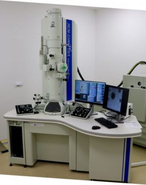
UHR TEM – Ultra High Reslution Transmission Electron Microscope JEM-2100Plus
- multi purpose transmission electron microscope for micro structure evaluation, which combines the proven JEM-2100 optic system with an advanced control system for enhanced ease of operation
- maximum accelerating voltage – 200kV
- guaranteed resolution – 0.14 nm (TEM lattice image)
- magnification – x30 to x800 000