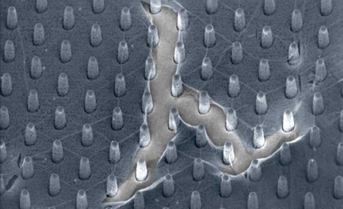
Mechanical deformation is capable of modifying the crystal structure and in turn also the (opto)electronic structure of 2D materials both globally and locally. It is thus crucial to monitor and control the deformation for any envisioned application of these materials, in a way that their unique properties are not compromised. On the other hand, their applicability can be even boosted by a smart choice of the deformation type and its level. For example, in graphene, uniaxial in-plane strain leads to symmetry breaking, elongating the C-C bonds in one direction and shortening them in the perpendicular one. This can – theoretically – lead to band gap opening when high enough elongation is reached, albeit the threshold is at the very limit of graphene’s predicted strain at failure. Bilayer graphene is more susceptible to the effects of stress: inhomogeneous uniaxial strain can lead to band-gap opening at much lower levels then those needed for monolayer graphene. Uniaxial out-of-plane compression in twisted bilayer graphene causes changes in the optical transition energies, otherwise controlled only by the misorientation angle between the two layers. In transition metal dichalcogenides, in-plane tension closes their band-gap, while compression opens it. Uniaxial out-of-plane compression in TMDCs closes the band-gap very quickly, and transition from semiconductor to semimetal is possible at quite low pressures. The stress can be relaxed by out-of-plane corrugations like ripples, wrinkles or folds, which alter the global mechanical properties as well as conductivity (for the worse), adhesion to the substrate (for the better) or local chemical potentials where large stress is accumulated. Sharp corrugations can even lead to phonon confinement.
We are looking both into the changes of the lattice under various deformations, ideally in-situ using Raman spectroscopy and photoluminescence, and into the possible ways of manipulating the structure permanently, mostly through substrate modification by thermal processing, patterning etc.
-
Pacakova B., Verhagen T., Bousa M., Hübner U., Vejpravova J., Kalbac M., Frank O. Mastering the Wrinkling of Self-supported Graphene. Scientific Reports 7(1), 10003 (2017). DOI:10.1038/s41598-017-10153-z (OPEN ACCESS)
-
del Corro E., Peña-Alvarez M.,Sato K., Morales-Garcia A., Bousa M., Mračko M., Kolman R.,Pacakova B., Kavan L., Kalbac M., Frank O.Fine tuning of optical transition energy of twisted bilayer graphene via interlayer distance modulation. Physical Review B 95(8), 085138 (2017). DOI:10.1103/PhysRevB.95.085138
-
Peña-Alvarez M., del Corro E., Morales García Á., Kavan L., Kalbac M., Frank O.Single Layer Molybdenum Disulfide under Direct Out-of-Plane Compression: Low-Stress Band-Gap Engineering.Nano Letters 15(5), 3139-3146 (2015). DOI:10.1021/acs.nanolett.5b00229
- Frank, O.; Tsoukleri, G., Riaz, I., Papagelis, K., Parthenios, J., Ferrari, A.C., Geim, A.K., Novoselov, K.S., Galiotis, C.: Development of a universal stress sensor for graphene and carbon fibres. Nature Communications 2, 255, (2011).DOI: 10.1038/ncomms1247(OPEN ACCESS)